
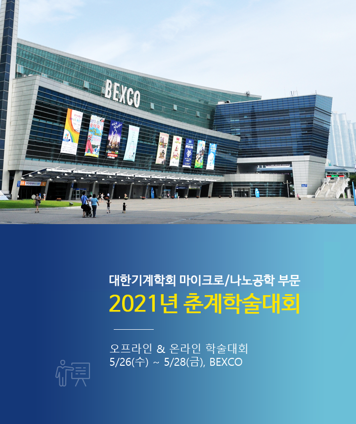

세션 트랙
|
PS1
포스터세션 - 마이크로/나노프린팅 및 패터닝 기술
|
PS1-1
Electrohydrodynamic jet printing for increasing the transparency of triboelectric nanogenerator
PS1-10
Nanotransfer printed transparent Ag nanomesh electrodes for flexible electronics
PS1-11
Study on the hot embossing process that can generate user-defined patterns in real time
PS1-13
A study on cost-effective process to fabricate nanostructure arrays on flexible substrates
PS1-14
파티클 혼합 레진을 이용한 메타홀로그램의 원스텝 제작
Single-step fabrication of metahologram using particle embedded resin
PS1-16
미세 Ag 전극 상 ZnO NW 하이브리드 구조체 성형 공정 기반 UV 센서 개발 All-solution-processible fabrication of micro- and nanopatterned device structures, exemplified by the ZnO nanowire-Ag hybrid flexible UV sensor
PS1-18
Mask-less fabrication of transparent conductive patterns with the electric field manipulated Ag microfibers
PS1-19
틸트나노각인 기반 가변경사 블레이즈 마이크로나노패턴 연속 직가공 Continuous direct machining of angle-tunable blazed micro- and nanopatterns by controlled axis-tilted nanoinscribing